Putting Manufacturing to the Test
Medical devices and life sciences instruments are commonly made up of hundreds – or sometimes thousands – of individual components, and often contain complex mechatronics, fluidics and optical subassemblies. The failure or inefficient operation of any one of these components can be enormously detrimental to device performance – even leading to complete device malfunction – which is why we verify the functionality of each individual component and subsystem before assembling and testing the completed instrument. Our team of knowledgeable electrical and mechanical test development engineers works hand in hand with our clients to ensure that any issues are picked up as early as possible, minimizing costly downstream reworking.
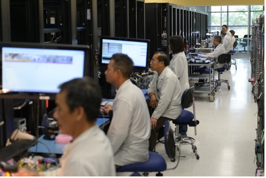
Function Test stations at Paramit.
How Do We Develop Our Testing Procedures?
We take a top-down approach to medical device testing here at Paramit, working closely with our clients to precisely determine the instrument functionalities that require verification. Any necessary test equipment and fixtures can either be supplied to us by our clients, or be fully designed and developed in house. Our team can also create custom software to automate testing protocols, analyze test results and communicate with completed devices. We are always keen to optimize processes in any way we can, which is why we will often suggest and implement operational adjustments to better aid production automation and scalability.
What Types of Testing Do We Offer?
Many medical devices and life sciences instruments include optical subassemblies that contain LEDs, lasers and cameras, all of which require precision positioning to ensure optimal performance. Similarly, the electrical continuity of a PCB assembly (PCBA), and the integrity of each of its electronic components, can be the difference between a perfectly functioning device and a scrap product. That’s why we employ the following test methods to identify any potential issues:
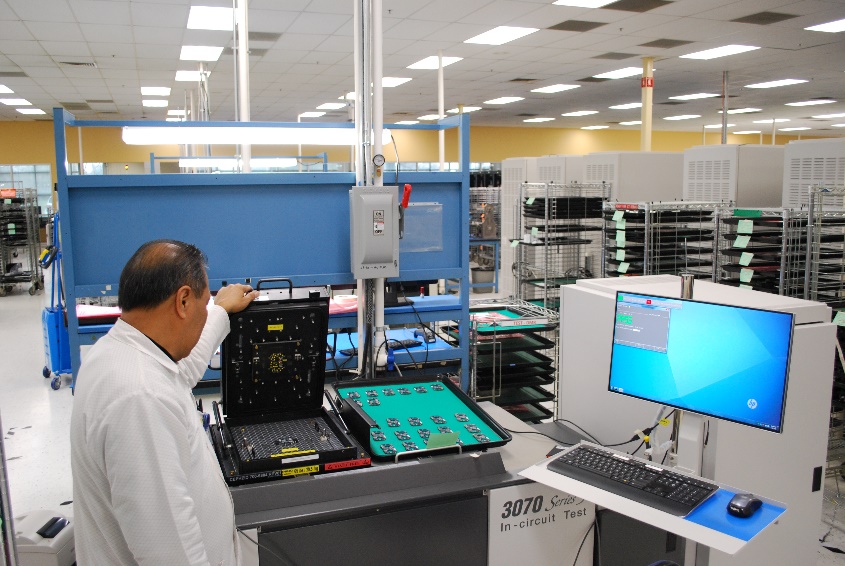
- In-circuit testing (ICT): Our expert team can design bespoke ICT procedures and fixtures to suit every PCBA, no matter the complexity. We use Keysight 3070 platforms to automatically detect defective traces and solder joints – including using boundary scan testing to verify board-level connection issues – as well as to identify faulty, missing or incorrectly installed components.
- X-ray verification: PCBAs that are not flagged during the ICT process can still contain sub-par solder joints, which are functional but prone to failure over time. That’s why we use Vitrox V810i automated X-ray inspection systems to assess the integrity of every solder joint in three dimensions, allowing us to identify any contacts that need reworking.
- Optical inspection: We inspect every PCBA using Koh Young Zenith 3D automated optical inspection (AOI) systems which use a series of cameras to automatically assesses solder joint integrity and identify missing components, alerting the team to any damage or defects.
- Functional testing: We validate the performance of each component – including PCBAs, pumps, heaters, power supplies and sensors – against its functional requirements and design specifications. Once component verification is complete, individual subassemblies are integrated into the final product using our innovative vPoke® mechanical assembly system.
- System testing: Following assembly, the final device undergoes rigorous system testing – usually via a client specified application programming interface – to ensure that all essential product features are operational. This can include testing everything from USB ports and LEDs to vacuum systems and robotic arms, depending on the instrument. This final phase of testing gives our clients an added layer of confidence that every device coming off the production line will work exactly as intended.
What Comes Next?
You’d be forgiven for thinking that this is where the process ends. However, we take every opportunity available to us to further streamline our processes here at Paramit. That’s why we analyze the treasure trove of data generated during the testing phase to identify and correct the root causes of assembly failures, allowing us to lower manufacturing costs and cycle times by fine tuning the production process.
What Does This Mean for Our Customers?
Our comprehensive testing solutions ensure that defects are identified as early as possible in the build process, minimizing the costly reworking of finished products that contain defective components or subsystems. The combination of ICT, X-ray verification and optical inspection – as well as subassembly and final device functional testing – allows us to maintain a failure rate of less than 10 defects per million parts produced. When combined with our fully traceable manufacturing processes, this gives our customers peace of mind that their devices will perform exactly as intended, every single time.
ICT (In-Circuit Test) station at Paramit.


